中文 | En
Products
Position: Home Products > Foundry services > > Chip Foundry Services
Chip Foundry Services
Chip Foundry
Pluto provides chip foundry service with close collaboration with whole world customers and the assurance that intellectual property is protected and respected.
 
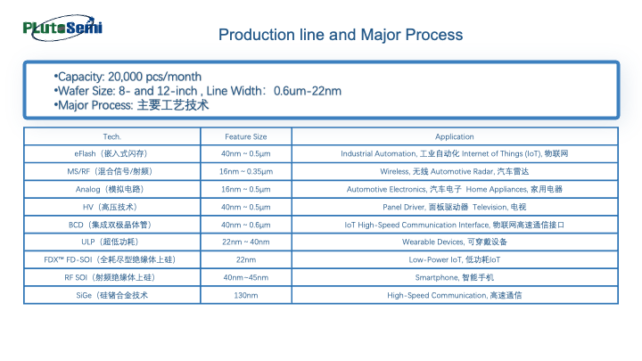
Pluto was known as PLUTOSEMI, a famous substrate manufacturer and solution provider, and has been operating for 10+ years. Our Chip foundry provides 6” (150mm) and 8” (200mm) wafer lines. we have 300 state-of-the-art semiconductor processing tools has marked a key milestone in our chip Foundry transformation. It has expanded Pluto’s capability to develop and manufacture sophisticated microdevices, biochips, and sensors.
 
Have your custom products outgrown the university environment, or do you require a level of customization at lower volumes that is not always supported in pure-play semiconductor foundries? Our team of experienced process engineers can help you manufacture your custom projects on 150- or 200-mm wafer diameters. We offer core competencies in the following areas:
· CMOS
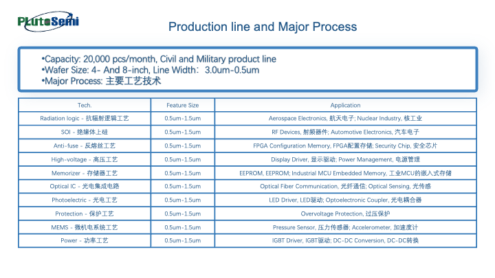
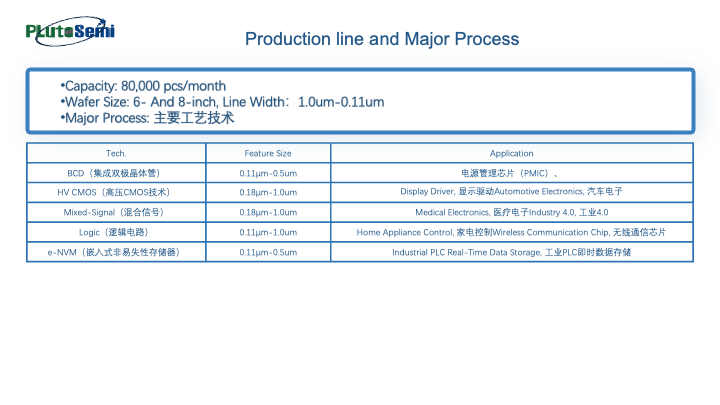
· Bipolar-CMOS-DMOS (BCD)
· Embedded Nonvolatile Memory (eNVM)
· Silicon-on-Insulator (SOI) high-voltage technologies
· Charge Coupled Devices (CCDs)
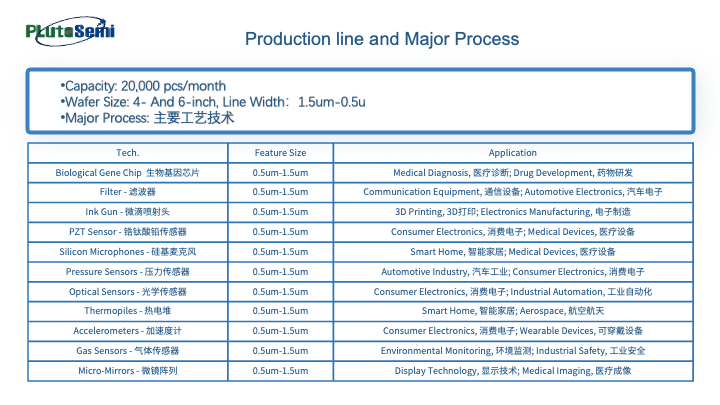
· Micro-Electrical Mechanical Systems (MEMS)

The semiconductor BCD (Bipolar-CMOS-DMOS) process is an integrated circuit manufacturing technology that integrates three different types of transistors—bipolar transistors (Bipolar), complementary metal-oxide-semiconductors (CMOS), and double diffused metal-oxide-semiconductors (DMOS)—onto a single chip. This process combines the high current driving capability of bipolar transistors with the low power consumption characteristics of CMOS circuits, as well as the high voltage and large current handling capabilities of DMOS devices.

The main features and applications of the BCD process are as follows:
1、Bipolar transistors (Bipolar): Used in analog circuits and high current applications because they can provide higher current gain.
2、Complementary metal-oxide-semiconductors (CMOS): Used in digital logic circuits due to their low power consumption and high integration.
3、Double diffused metal-oxide-semiconductors (DMOS): Used in power electronic devices, such as high voltage or large current switches, because they can handle higher voltages and currents.

The key advantages of the BCD process include:
1、Versatility: Multiple functions, such as analog, digital, and power circuits, can be integrated on the same chip.
2、Energy efficiency: By combining the advantages of bipolar transistors and CMOS, it achieves circuit designs with higher energy efficiency.
3、Integration: High integration reduces the chip area and lowers costs.
4、Performance: It can provide high current driving capability and the ability to handle high voltages.

The BCD process is widely used in the following fields:
1、Automotive electronics: Power management, motor control, body electronics, and entertainment systems in cars.
2、Consumer electronics: Power management in smartphones, tablets, and other portable devices.
3、Industrial applications: Industrial automation, power electronics, and control systems.
As technology advances, the BCD process is also evolving, with developments like BCD5, BCD6, etc., offering higher voltage and power handling capabilities, as well as improved performance and energy efficiency.


● Available                        ★Indude SOI Process
Tech. BCD HV CMOS Mixed-Signal Logic e-NVM
0.13μm/0.11μm    
0.18μm/0.153μm
0.25μm      
0.35μm    
0.5μm ● ★
>0.5μm    
>1.0μm    
MEMS Pressure sensor,Microphone sensor,Photoelectric MEMS and Thermopiles sensor are available.
Accelerometer,Gas sensorand Micro-mirrorare under development.
Special Device APD/SPAD are underdevelopment.

★Advanced  BCD  Available       ▲Advanced BCD Developing       ●HV /UHV BCDAvailable       ⊙Include SOI Process
  0.11μm 0.153μm 0.18μm 0.25μm  0.5μm 0.8μm  1.0μm
12V      
18V      
24V      
30V      
40V    
60V          
80V            
120V       ●⊙    
200V       ●⊙
600V         ●⊙
700V        
1200V            

Sales Engineer:Lance Xie
Phone:+86 138 2505 8605
Email:Lance@plutosemi.com
Sub 1: PlutoChip Co., Ltd    -Discrete Devices and Integrated Circuits-    www.plutochip.com
Sub 2: PlutoSilica Co., Ltd   -Silicon Wafer and Glass Wafer Manufactory-
Copyright © 2020 | PlutoSemi Co., Ltd | All Rights Reserved