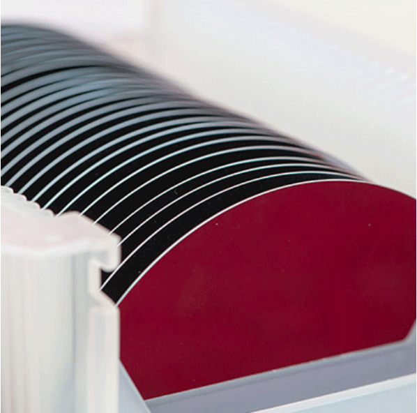
About zone-fused silicon wafers
一、The basic principle of zone-melted silicon wafers
Zone Melting, also known as zone melting, is a technology that uses local heating to redistribute the impurities in the silicon rod at the solid-liquid interface, so as to achieve the purpose of purification. During zone melting, a high-frequency induction coil moves slowly along the silicon rod, creating a narrow melting zone on the silicon rod. Due to the different solubility of impurities in liquid silicon and solid silicon, when the molten zone moves, the impurities are gradually pushed to one end of the silicon rod as the molten zone moves, thus achieving the purification of silicon. After multiple times of zone melting and purification, high-purity silicon rods can be obtained, and then they can be cut, grinded, polished and other processes to make zone melt silicon wafers.
二、Characteristics of zone-fused silicon wafers
1. High purity: Through zone melting technology, the content of impurities in silicon wafers can be reduced to very low levels, such as phosphorus, boron and other impurities can reach the ppb (parts per billion) level, which makes zone melting silicon wafers have excellent electrical properties.
1. High resistivity: Due to the low impurity content, the resistivity of zone-melt silicon wafers is much higher than that of general Straight-pull silicon wafers (CZ wafers), typically reaching 1000 - 10000 Ω・cm, or even higher. This high resistivity gives zone-melt silicon wafers a unique advantage in the manufacture of high-voltage, high-power semiconductor devices.
1. Good crystal quality: During the process of zone melting, silicon atoms can form a relatively perfect lattice structure during crystallization, which reduces crystal defects, such as dislocations and lamination faults. This enables zone-fused silicon wafers to maintain stable performance even under extreme working conditions such as high temperature and high pressure.
三、Application fields of zone-fused silicon wafers
1. Power semiconductor devices: In the manufacture of high-voltage power transistors (such as IGBTs, MOSFETs, etc.), the high resistivity and good crystal quality of zone-fused silicon wafers can effectively reduce the on-resistance of the device, improve the voltage resistance and switching speed of the device, and are widely used in electric vehicles, smart grids, industrial frequency conversion and other fields. For example, in the charging piles and on-board chargers of electric vehicles, the use of zone-fused silicon wafers in IGBT modules can improve charging efficiency and reduce energy loss.
1. Sensor field: zone-fused silicon wafers are used to manufacture pressure sensors, acceleration sensors, etc., and its high purity and stable crystal structure help to improve the sensitivity and accuracy of the sensor, ensure the reliable operation of the sensor under different environmental conditions, and play an important role in automotive electronics, aerospace and other fields.
1. Optoelectronic devices: In the manufacture of some optoelectronic devices with extremely high requirements for material purity and crystal quality, such as infrared detectors and laser diodes, zone melt silicon wafers are also used. It can provide a stable performance foundation for optoelectronic devices, and improve the luminous efficiency and detection sensitivity of optoelectronic devices.