Position:
Home News >
Company News > >
Straight-pull wafers: the cornerstone of the semiconductor industry
Straight-pull wafers: the cornerstone of the semiconductor industry
一、Definitions and Overview
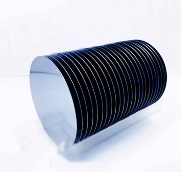
Czochralski Silicon Wafer (CZ wafer) is a round thin wafer made by growing a monocrystalline silicon rod from a silicon melt by the Czochralski method, and then going through a series of precision processing processes such as cutting, grinding, and polishing. As the core carrier of semiconductor materials, Zyopull silicon wafers occupy a pivotal position in the modern electronics industry and are the basic materials for many semiconductor products such as integrated circuits, discrete devices, and sensors.
二、Manufacturing process
(一)Preparation of raw materials
The first step is to produce high-purity polysilicon, which typically requires a purity of more than 99.9999% or more. The quality of these polysilicons, which are used as raw materials for growing monocrystalline silicon, directly affects the quality of the final Zhizo-pull wafers.
(二)Monocrystalline silicon is grown by the Zyopull method
The polysilicon is placed in a quartz crucible and heated to about 1420°C in a monocrystalline furnace to melt completely. Then, a seed crystal is immersed in the silicon melt, slowly rotated and pulled upwards, while controlling parameters such as temperature and pulling speed. Under the induction of the seed crystal, the silicon atoms will grow layer by layer on the seed crystal according to a certain lattice arrangement, and finally form a large-diameter monocrystalline silicon rod. This process requires precise control of the thermal field, temperature gradient, drawing rate, and rotational speed of the crystal to ensure that the grown monocrystalline silicon rods have a uniform crystal structure and low defect density.
(三)Wafer processing
- Cutting: The grown monocrystalline silicon rod is cut into silicon wafers of a certain thickness with an internal circle cutting machine or a wire cutting machine. During the cutting process, attention should be paid to controlling the cutting accuracy and surface quality to reduce cutting damage and warpage.
- Grinding: Grinding the cut silicon wafer to remove the surface damage layer generated during the cutting process, so that the surface of the silicon wafer is smooth and smooth, and meets the specified thickness tolerance requirements.
- Polishing: Through chemical mechanical polishing (CMP) and other technologies, the flatness and finish of the surface of the silicon wafer are further improved, so that the surface roughness reaches the nanometer level, which meets the extremely high flatness requirements of the subsequent semiconductor manufacturing process on the surface of the silicon wafer.
- Cleaning: After multiple cleaning processes, the impurities, particles, organic matter and other contaminants remaining on the surface of the silicon wafer are removed to ensure the cleanliness of the surface of the silicon wafer and provide a good foundation for the subsequent chip manufacturing process.
三、Characteristic
(一)Crystal structure
The highly ordered crystal structure of the Zzozopull silicon wafer gives the silicon wafer excellent electrical properties, such as high carrier mobility, low resistivity, etc., which is conducive to the transport of electrons in the silicon wafer, thus ensuring the efficient operation of semiconductor devices.
(二)Electrical performance
Silicon is an intrinsic semiconductor, and by precisely controlling the type and concentration of doped elements (such as boron, phosphorus, etc.), the electrical properties of Zzopull silicon wafers can be adjusted to meet the needs of different types of semiconductor devices. For example, P-type silicon wafers can be prepared by doping boron, and N-type silicon wafers can be obtained by doping phosphorus, and these different types of silicon wafers are widely used in various integrated circuits and discrete devices.
(三)Thermal performance
Silicon has good thermal stability and high thermal conductivity, and is able to maintain stable physical and electrical properties over a certain temperature range. During the operation of semiconductor devices, the heat generated can be effectively conducted out through the silicon wafer to ensure the normal operation of the device and prevent performance degradation or damage caused by overheating.
(四)Mechanical properties
Straight-pull silicon wafers have certain mechanical strength and hardness, and can withstand various machining and operations in the semiconductor manufacturing process, such as lithography, etching, ion implantation, etc., etc. At the same time, its good flatness and dimensional accuracy also ensure that each layer of thin film and device structure can be accurately fabricated on the surface of the silicon wafer during the chip manufacturing process.
四、Fields of application
(一)IC
In integrated circuit manufacturing, Zyopull silicon wafers are the key materials for the manufacture of various microprocessors, memory chips, logic chips, etc. With the continuous progress of semiconductor technology, the integration of chips is getting higher and higher, and the requirements for the size, flatness, and defect density of Zzo-pull silicon wafers are becoming more and more stringent. For example, today's advanced integrated circuit manufacturing processes have adopted 12-inch or larger size of straight-pull silicon wafers to improve chip production efficiency and reduce costs.
(二)Discrete devices
Discrete devices such as diodes, transistors, thyristors, and power MOSFETs are widely used in power electronics, automotive electronics, communications, and other fields. As the basic material of these discrete devices, the performance of Zzolabio silicon wafers directly affects the performance and reliability of discrete devices. For example, in power semiconductor devices, silicon wafers are required to have characteristics such as low resistivity and high breakdown voltage to meet the needs of high-power and high-efficiency applications.
(三)sensor
Silicon-based sensors are an important part of modern sensor technology, such as pressure sensors, accelerometers, gyroscopes, etc. Due to its good mechanical and electrical properties, Zolizo-pull silicon wafers are ideal for the manufacture of sensitive components for various sensors. Through microelectromechanical systems (MEMS) technology, various microstructures and sensor chips can be accurately manufactured on silicon wafers to achieve high-precision detection and conversion of physical and chemical quantities.