A detailed introduction to sapphire epitaxial wafers
一、Definition and basic concepts
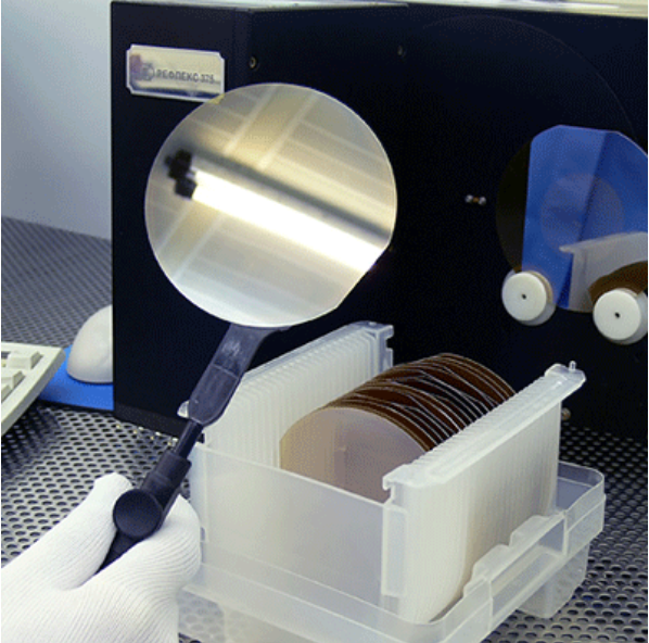
Sapphire epitaxial wafer is a thin film of semiconductor material with specific crystal structure and properties formed by epitaxial growth technology on a sapphire substrate. Among them, sapphire (Al₂O₃) has become an ideal substrate material due to its good chemical stability, high hardness, high melting point, and lattice constant matched to a variety of semiconductor materials. Epitaxial growth is a technology that grows a new layer of single crystal thin film on a single crystal substrate, and the newly grown film matches the lattice structure of the substrate to obtain high-quality semiconductor thin film materials.
二、Manufacturing process
1.Chemical Vapor Deposition (CVD): This is currently the most commonly used method for manufacturing epitaxial wafers for sapphire. Under the action of high temperature and catalyst, gaseous raw materials such as silicon and carbon undergo chemical reactions on the surface of sapphire substrate, and the atoms are gradually deposited and arranged according to a certain lattice structure, so as to grow an epitaxial layer. This method enables precise control of the thickness, composition, and doping concentration of the epitaxial layer, resulting in the preparation of high-quality epitaxial wafers.
2.Molecular beam epitaxy (MBE): In an ultra-high vacuum environment, atoms or molecular beams such as silicon and germanium are evaporated onto the surface of the sapphire substrate, and the atoms grow layer by layer on the surface of the substrate to form an epitaxial layer. This method has a low growth rate, but can achieve precise control at the atomic level, and can prepare epitaxial layers with atomic-level flatness and extremely thin thickness, which is often used to prepare sapphire epitaxial wafers in high-end scientific research and special application fields.
三、Fields of application
1.LED lighting: It is one of the main application areas of sapphire epitaxial wafers. A gallium nitride (GaN) epitaxial layer is grown on a sapphire substrate to create LED chips that emit highly efficient blue light and can be illuminated with phosphor conversion. Due to the good heat dissipation performance of sapphire and the lattice matching with GaN, the LED chips have excellent performance in terms of luminous efficiency, stability and lifetime.
2.Power electronics: Silicon carbide (SiC) epitaxial layers grown on sapphire epitaxial wafers can be used to manufacture high-power, high-frequency electronic devices such as MOSFETs, IGBTs, etc. These devices have important applications in electric vehicles, smart grids, new energy power generation and other fields, which can improve power conversion efficiency and reduce energy consumption.
3.Optical communication: In the field of optical communication, optoelectronic devices based on sapphire epitaxial wafers, such as lasers and detectors, can achieve high-speed and long-distance optical signal transmission. For example, lasers made with an epitaxial layer of indium gallium arsenic phosphorus (InGaAsP) grown on a sapphire substrate can be used as an optical emission module in fiber optic communication systems to meet the growing demand for high-speed data transmission.
四、advantage
1.Excellent physical properties: Sapphire has the characteristics of high hardness, high melting point and good chemical stability, which makes the sapphire epitaxial wafer maintain good performance in harsh environments such as high temperature, high voltage and strong radiation, and improves the reliability and service life of the device.
2.Good optical properties: Sapphire has a high transmittance to ultraviolet, visible and infrared rays, which makes sapphire epitaxial wafer-based optoelectronic devices have advantages in optical applications, such as LED lighting, optical communication and other fields, which can improve the emission and transmission efficiency of light.
3.Matching with a variety of semiconductor materials: The lattice constant of sapphire has a certain degree of matching with a variety of semiconductor materials such as gallium nitride and silicon carbide, which can grow a high-quality epitaxial layer on it, which provides the possibility for the development of new semiconductor devices.
五、Trends
1.Large-size: With the increasing market demand for sapphire epitaxial wafers, large-size sapphire epitaxial wafers can improve production efficiency and reduce costs. Therefore, the research and development of large-size sapphire substrates and epitaxial growth technologies to achieve the production of larger-size sapphire epitaxial wafers is one of the future development trends.
2.Combination with new materials: Exploring the combination with new semiconductor materials, such as two-dimensional materials, developing new optoelectronic devices with higher performance, and expanding the application field of sapphire epitaxial wafers are also one of the future research directions.