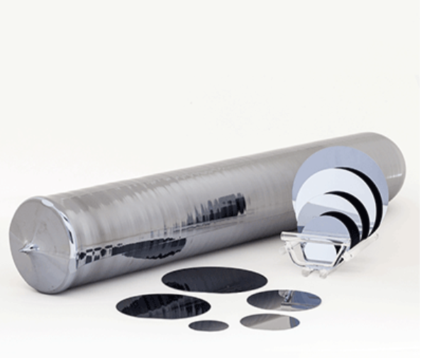
Silicon wafer manufacturing process
1. Silicon wafer manufacturing process
The silicon wafer manufacturing process usually includes the following main steps:
1.1 Crystal Growth
method:Commonly used straight pull method(Czochralski)or Zone melting method(Float Zone)。
process:High-purity polycrystalline silicon is placed in a quartz crucible and heated to melt, and then a single crystal silicon rod is slowly pulled out by rotating the seed crystal.
result:Forming cylindrical single crystal silicon ingot
1.2 Ingot Processing
process:
Cropping:Cut off the irregular parts of the silicon rod head and tail
Grinding:The outer diameter of the silicon rod is ground to the standard diameter.
Notching:A positioning surface (flat or notch) is cut on the silicon rod for crystal orientation positioning in subsequent processes.
1.3 Slicing
The silicon rod is sliced into thin slices with uniform thickness.
1.4 Edge Rounding
Purpose:Grind off the sharp corners of the silicon wafer edges after slicing to prevent fragments or cracks in subsequent processes.
1.5 Lapping/Grinding
Purpose:Remove the damaged layer on the surface of silicon wafers after slicing and improve thickness uniformity.
1.6 Etching
Purpose:Surface damage and impurities produced during the grinding process are removed by chemical etching.
1.7 Polishing
Purpose:Make the surface of silicon wafer mirror smooth.
1.8 Oxidation(If the customer requires oxidation thickness)
1.9 Cleaning
Purpose:Remove particles and contaminants from the surface of polished silicon wafers.
1.10 Inspection & Packaging
Inspection:The surface quality, thickness, resistivity and other parameters of silicon wafers are tested.
Packaging:Qualified silicon wafers are packaged and labeled for shipment.
(二)Wafer parameters
2. Determination of silicon wafer parameters at different stages
2.1 Parameters determined during crystal growth
Oxygen Concentration :The oxygen content mainly comes from the dissolution of the quartz crucible during the growth of the silicon rod. The oxygen content of the Czochralski silicon rod is usually higher.
Carbon Concentration :The carbon content mainly comes from the pollution in the polysilicon raw materials or the growth environment, and carbon impurities are introduced during the growth process of silicon rods.
EPD (Etch Pit Density)
OSF (Oxidation-Induced Stacking Faults):OSF is mainly related to crystal defects during the growth of silicon rods, and subsequent heat treatment (such as oxidation process) may further affect OSF.
Crystal Orientation :like(100)、(111)etc.,Determined by the crystal orientation of the seed crystal.
Resistivity :Determined by the doping concentration, which is determined during the silicon rod growth process.
Conductivity Type :P-type or N-type, determined by the doping element (such as boron or phosphorus).
2.2 Parameters determined when slicing the morphology
Thickness:The thickness of the silicon wafer is preliminarily determined during slicing.
TTV, Total Thickness Variation:It is initially determined after slicing, but further optimized by subsequent grinding and polishing.
Bow/Warp :Determine when basic slicing
2.3 Parameters determined after chamfering
Diameter, chamfer shape(R22、R150、R130 22Deg etc.)
2.4 Parameters determined by the grinding process
Roughness:Initial improvement after grinding, but final determination by polishing.
TTV(Thickness uniformity):This is corrected after grinding, but is ultimately determined by polishing.
2.5 Parameters determined by the polishing process
Roughness
TTV(Thickness uniformity)
Surface Quality :Such as surface defects (such as orange peel texture, chicken claw prints, doping rings), particle contamination, surface metal impurity content, etc., which are determined by polishing and cleaning.
Local flatness:Such as SFQR and STIR, which are determined by polishing.
TIR flatness: Determined by polishing
2.6 Parameters determined by the oxidation process
The thickness of the oxide layer is determined by the oxidation process, which is usually performed after the silicon wafer is polished.