1. Introduction
In the wave of rapid development of modern science and technology, semiconductor technology, as a key force supporting innovation in many fields, is of self-evident importance. As the core material in the semiconductor manufacturing process, the epitaxial wafer is like a bright pearl, shining with unique light on the stage of the semiconductor industry. It not only determines the performance and quality of semiconductor devices, but also plays a vital role in promoting the development of the entire electronic information industry.
2. Definition and principle of epitaxial wafer
(1) Definition
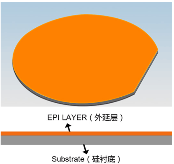
Epiwafers are formed by growing a layer of single-crystal semiconductor thin film with specific electrical, optical and structural properties on the surface of substrate materials (such as silicon, silicon carbide, sapphire, etc.) through epitaxial growth technology. The properties of this epitaxial layer can be precisely controlled and adjusted according to different application requirements, thus laying the foundation for the manufacture of various high-performance semiconductor devices.
(2) Principle of epitaxial growth
The basic principle of epitaxial growth is to decompose the gaseous semiconductor source material through chemical reaction in a high-temperature, low-pressure reaction environment, and make its atoms or molecules adsorb, migrate and deposit on the substrate surface, gradually forming an orderly single-crystal thin film. Common epitaxial growth techniques include chemical vapor deposition (CVD), molecular beam epitaxy (MBE), etc.
1. Chemical vapor deposition (CVD): In the CVD process, gaseous compounds containing semiconductor elements (such as silane SiH₄, trimethylgallium Ga (CH₃)₃, etc.) are introduced into the reaction chamber together with a carrier gas (such as hydrogen H₂). Under high temperature conditions, the gaseous compounds undergo a decomposition reaction to release semiconductor atoms, which are deposited on the substrate surface and gradually form an epitaxial layer. Depending on the reaction conditions and equipment structure, CVD can be divided into atmospheric pressure chemical vapor deposition (APCVD), low pressure chemical vapor deposition (LPCVD) and plasma enhanced chemical vapor deposition (PECVD).
2. Molecular beam epitaxy (MBE): MBE is an epitaxial growth technology performed in an ultra-high vacuum environment. In the MBE system, an atomic beam or molecular beam of semiconductor elements is directly sprayed onto the substrate surface through a precisely controlled evaporation source. Since the mean free path of atoms is very long in an ultra-high vacuum environment, they can be adsorbed and arranged in an orderly manner on the substrate surface, thereby growing a high-quality epitaxial layer. MBE technology has the advantages of low growth rate and high atomic-level growth control accuracy, and is particularly suitable for manufacturing semiconductor devices with complex structures and high performance requirements, such as quantum well lasers, high electron mobility transistors (HEMTs), etc.
3. Manufacturing process of epitaxial wafers
The manufacturing of epitaxial wafers is a complex and delicate process that requires highly precise equipment and strict process control. The following are the main steps in general epitaxial wafer manufacturing:
(1) Substrate preparation: Selecting a suitable substrate material is the first step in epitaxial wafer manufacturing. The quality and characteristics of the substrate material have an important influence on the growth quality of the epitaxial layer. Common substrate materials include silicon (Si), silicon carbide (SiC), sapphire (Al₂O₃), etc. Before use, the substrate needs to be strictly cleaned and polished to remove surface impurities and defects to obtain a smooth and flat surface.
(2)Epitaxial growth: Place the pre-treated substrate into the epitaxial growth equipment, and select the appropriate epitaxial growth technology and process parameters according to the material and characteristics of the required epitaxial layer. During the growth process, the flow rate, temperature, pressure and other parameters of the reaction gas are precisely controlled to ensure that the epitaxial layer grows according to the predetermined requirements. For example, when growing silicon epitaxial wafers, silane is usually used as a silicon source, and the growth rate and thickness of the epitaxial layer are controlled by controlling the flow rate and reaction temperature of silane.
(3) Quality inspection: After the epitaxial growth is completed, the epitaxial wafer needs to be fully inspected for quality. The inspection items include the thickness, resistivity, carrier concentration, and crystal structure integrity of the epitaxial layer. Commonly used inspection methods include scanning electron microscopy (SEM), atomic force microscopy (AFM), secondary ion mass spectrometry (SIMS), Hall effect measurement, etc. Through these inspection methods, defects and problems in the epitaxial wafer can be discovered in time, and the production process can be adjusted and optimized.
(4)Cutting and packaging: Epitaxial wafers that have passed the quality inspection are cut into chips of different sizes according to actual application requirements. Then, the chip is packaged to protect it from the external environment and provide electrical connection and mechanical support for the chip. The packaged chip can be used as a semiconductor device in various electronic devices.
4. Types of epitaxial wafers
According to the different substrate materials and epitaxial layer materials, epitaxial wafers can be divided into many types, the most common ones are as follows:
(1)Silicon epitaxial wafer: an epitaxial wafer with silicon as the substrate material to grow the silicon epitaxial layer. Silicon epitaxial wafers are the most widely used epitaxial wafer type at present, mainly used to manufacture integrated circuits (ICs), power semiconductor devices (such as MOSFET, IGBT, etc.), sensors, etc. Due to the good electrical properties, mature manufacturing processes and low costs of silicon materials, silicon epitaxial wafers occupy a dominant position in the semiconductor industry.
(2) Compound semiconductor epitaxial wafers: epitaxial wafers with compound semiconductor materials (such as silicon carbide SiC, gallium nitride GaN, gallium arsenide GaAs, etc.) as substrates or epitaxial layer materials. Compound semiconductors have better electrical properties than silicon, such as high electron mobility, high breakdown electric field, high thermal conductivity, etc. Therefore, compound semiconductor epitaxial wafers have unique advantages in high-frequency, high-power, high-temperature and other application fields. For example, silicon carbide epitaxial wafers are mainly used to manufacture high-voltage power devices, which can be widely used in electric vehicles, smart grids, industrial control and other fields; gallium nitride epitaxial wafers have important applications in radio frequency communications, LED lighting, power electronics and other fields.
(3) Silicon on insulator (SOI) epitaxial wafer: a special epitaxial wafer with a silicon epitaxial layer grown on an insulating substrate (such as silicon dioxide SiO₂). SOI epitaxial wafers have good isolation performance and low power consumption characteristics, which can effectively improve the performance and reliability of integrated circuits and reduce the power consumption and cost of chips. SOI epitaxial wafers are mainly used in high-performance microprocessors, radio frequency integrated circuits, sensors and other fields.
5. Application fields of epitaxial wafers
As a key material for semiconductor manufacturing, epitaxial wafers are widely used in various electronic information fields and have played an important role in promoting the development of modern science and technology. The following are the main application areas of epitaxial wafers:
(1) Integrated Circuits (ICs): Integrated circuits are the core of the modern electronic information industry, and epitaxial wafers play a vital role in IC manufacturing. By growing different types of epitaxial layers on silicon epitaxial wafers, various high-performance transistors, diodes and other devices can be manufactured, thereby realizing complex logic circuits and storage circuit functions. With the continuous development of integrated circuit technology, the quality and performance requirements of silicon epitaxial wafers are becoming higher and higher, such as requiring the epitaxial layer to have higher purity, more precise thickness control and lower defect density.
(2) Power semiconductor devices: Power semiconductor devices are mainly used in the field of power conversion and control, such as motor drive for electric vehicles, power transmission and distribution of smart grids, and power management of industrial automation equipment. Compound semiconductor epitaxial wafers such as silicon carbide and gallium nitride have the characteristics of high breakdown electric field, high electron mobility and high thermal conductivity, and can manufacture power semiconductor devices with higher power density, higher efficiency and lower energy consumption, so they have been widely used in the field of power semiconductors.
(3) Optoelectronic devices: Optoelectronic devices are devices that use the principle of interaction between light and matter to achieve mutual conversion between optical signals and electrical signals, such as light-emitting diodes (LEDs), laser diodes (LDs), photodetectors, etc. Epitaxial wafers are key materials in the manufacture of optoelectronic devices. For example, in LED manufacturing, by growing gallium nitride epitaxial layers on sapphire or silicon carbide substrates, efficient LED chips can be manufactured, which are widely used in lighting, display, car taillights and other fields; in laser diode manufacturing, molecular beam epitaxy and other technologies are used to grow epitaxial layers with specific structures, which can achieve high-power and high-efficiency laser emission, and are used in optical communications, laser processing, medical and other fields.
(4) Sensors: Sensors are devices that can sense external physical quantities, chemical quantities or biomass information and convert them into electrical signal outputs. Epitaxial wafers are also widely used in sensor manufacturing. For example, silicon epitaxial wafers can be used to manufacture pressure sensors, acceleration sensors, etc.; compound semiconductor epitaxial wafers can be used to manufacture gas sensors, ultraviolet sensors, etc. By growing an epitaxial layer with specific functions on the substrate, the sensor can achieve high-sensitivity detection and precise measurement of different signals.
6. Market development trend of epitaxial wafers
With the rapid development of the global electronic information industry, the demand for epitaxial wafers continues to grow, driving the epitaxial wafer market to continue to expand. At the same time, with the continuous innovation of semiconductor technology and the continuous expansion of application fields, the epitaxial wafer market has also shown some new development trends:
(1) Technology innovation driven: In order to meet the ever-increasing performance requirements of semiconductor devices, epitaxial wafer manufacturing technology will continue to innovate. On the one hand, traditional epitaxial growth technology will continue to be optimized and improved to improve the quality and growth efficiency of epitaxial layers; on the other hand, new epitaxial growth technologies and material systems will continue to emerge, such as epitaxial growth technology based on atomic layer deposition (ALD), new two-dimensional material epitaxial wafers, etc., bringing new opportunities for the development of the semiconductor industry.
(2) The demand for compound semiconductor epitaxial wafers is growing rapidly: With the rapid development of emerging industries such as 5G communications, new energy vehicles, and industrial Internet, the demand for high-frequency, high-power, and high-temperature semiconductor devices has increased sharply, driving the rapid growth of compound semiconductor epitaxial wafer markets such as silicon carbide and gallium nitride. It is expected that the market share of compound semiconductor epitaxial wafers will continue to expand in the next few years, becoming one of the main driving forces for the growth of the epitaxial wafer market.
(3) The trend of large-size is obvious: In the field of semiconductor manufacturing, in order to improve production efficiency and reduce costs, the size of epitaxial wafers continues to increase. At present, 8-inch and 12-inch silicon epitaxial wafers have become mainstream products in the market, and with the continuous advancement of technology, 18-inch or even larger silicon epitaxial wafers are also in the research and development and trial production stage. For compound semiconductor epitaxial wafers, such as silicon carbide epitaxial wafers, although the current large-size technology still faces some challenges, it is also moving towards a larger size to meet the market demand for low-cost, high-performance semiconductor devices.
(4) Increasingly fierce market competition: With the continuous expansion of the epitaxial wafer market, more and more companies are entering this field, and market competition is becoming increasingly fierce. On the one hand, traditional semiconductor material companies continue to increase R&D investment to improve product quality and market competitiveness; on the other hand, some emerging companies are also emerging in the market with advanced technology and innovative business models. In the fierce market competition environment, companies need to continuously improve their technical level, optimize product structure, and reduce production costs to occupy a favorable position in the market.