In the process of continuous evolution of semiconductor technology, Silicon-on-Insulator (SOI) has become a key force in promoting the development of integrated circuits with its unique structure and excellent performance, and occupies an increasingly important position in the modern electronics industry.
1. Basic Concepts and Structure
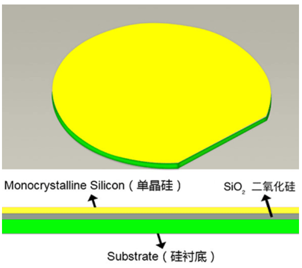
Silicon-on-Insulator (SOI) is a special semiconductor material structure that separates the top silicon from the bottom silicon substrate with an insulating layer (usually silicon dioxide). This "silicon-insulator-silicon" sandwich structure fundamentally changes the electrical properties of traditional silicon-based semiconductors. The top silicon is used as an active layer to build semiconductor devices such as transistors; the middle insulating layer, like an "isolation wall" for electrical signals, effectively reduces parasitic capacitance and leakage between devices; the bottom silicon substrate provides mechanical support for the entire structure.
Compared with traditional bulk silicon, the SOI structure greatly reduces the capacitance of the device, which means faster signal transmission and lower power consumption. For example, in high-frequency circuit applications, the parasitic capacitance of traditional bulk silicon transistors can cause signal delays and energy loss, while SOI transistors can significantly reduce this effect, making circuit operation more efficient.
2. Manufacturing process
1. Oxygen implantation isolation (SIMOX) process: By injecting a high dose of oxygen ions into the silicon substrate, a silicon dioxide insulating layer is formed at a specific depth. After high-temperature annealing, the injected oxygen ions react with silicon to generate a continuous and high-quality silicon dioxide layer, on which a high-quality silicon layer is grown as an active layer. This process can accurately control the thickness of the insulating layer and the silicon layer, has high repeatability, is suitable for large-scale production, and is often used to manufacture high-end integrated circuits that require extremely high quality and thickness consistency of the insulating layer.
2. Bonding and grinding technology (BESOI): First grow or deposit a silicon dioxide insulating layer on a silicon wafer, and then bond this silicon wafer to another silicon wafer. After bonding, most of the bottom silicon wafer is removed through grinding and polishing processes, leaving only a thin top silicon as the active layer. This process is highly flexible and can select different types of silicon wafers for bonding according to different needs. It is widely used in some fields that require high cost control and process flexibility.
3. Performance advantages
1. Low power consumption: Due to the isolation effect of the insulating layer, the leakage current of SOI devices is greatly reduced. Taking microprocessors as an example, after adopting SOI technology, the static power consumption of the chip can be reduced by about 30%-50%. This is of great significance in the field of mobile electronic devices, which can effectively extend battery life and meet people's needs for device portability and long battery life.
2. High integration: The SOI structure reduces the parasitic effects between devices, allowing transistors to be arranged more closely, thereby improving the integration of the chip. Under the same chip area, SOI technology can integrate more transistors and improve the computing power and functional complexity of the chip. For example, in high-end FPGA (field programmable gate array) chips, SOI technology can achieve higher logic density and enhance the parallel processing capability of the chip.
3. Strong radiation resistance: SOI performs well in fields with harsh radiation environments such as aerospace and military. The insulating layer can effectively block radiation particles, reduce their impact on the electrical performance of transistors, and reduce the risk of circuit failure caused by single particle effects. For electronic equipment like satellites, the use of SOI technology can improve the reliability and stability of the system in the space radiation environment.
4. High-speed operation: Low parasitic capacitance and resistance make the switching speed of SOI devices faster and the signal transmission delay shorter. In the RF circuit of 5G communication base stations, RF switches and amplifiers using SOI technology can achieve higher frequency response and data transmission rate, ensuring the high-speed communication performance of 5G networks.
4. Application fields
1. Mobile communications: In the chips of smart phones, base stations and other devices, SOI is widely used in key components such as RF front-ends and baseband processors. It can improve signal processing capabilities, reduce power consumption, help achieve the high-speed and low-latency requirements of 5G and even future 6G communications, and improve users' communication experience.
2. Automotive electronics: With the development of intelligent and electrified vehicles, the reliability and performance requirements of electronic systems are getting higher and higher. SOI is used in automotive power electronics, sensor interface circuits, etc. It can work stably in complex environments such as high temperature and vibration, such as the battery management system of electric vehicles and the radar sensor circuit of autonomous driving, ensuring the safe and reliable operation of automotive electronic systems.
3. Internet of Things (IoT): Among the massive IoT devices, SOI provides support for various sensor nodes and microcontrollers with its advantages of low power consumption, small size and high integration. These devices usually rely on batteries for power supply. SOI technology can extend the service life of the equipment while achieving multi-functional integration, meeting the development trend of miniaturization and intelligence of IoT devices.
4. Aerospace: Aerospace equipment such as satellites and aircraft have almost stringent requirements on the performance and reliability of electronic equipment. SOI's radiation resistance, high speed and low power consumption make it an indispensable material in aerospace electronic systems. From satellite onboard computers to aircraft navigation systems, SOI technology can be seen.
5. Development Status and Challenges
At present, SOI technology has been widely used in the global semiconductor industry, and many internationally renowned semiconductor companies have laid out SOI product lines. However, the development of SOI technology also faces some challenges. On the one hand, the complex manufacturing process leads to high costs, limiting its large-scale application in some cost-sensitive fields; on the other hand, as the chip process develops to more advanced nodes, higher requirements are placed on the quality and performance of SOI materials, such as thinner and more uniform insulation layers and silicon layer control, higher crystal quality, etc., which require continuous research and development of new processes and new equipment to meet.