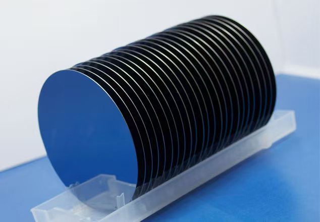
The development trend of Czochralski-pull wafers wafers
Technological innovation leads development
(1)The process of large-size development is accelerating
In order to improve production efficiency and reduce costs, the large size of straight-pull silicon wafers has become an important trend. In the photovoltaic field, the size of silicon wafers has gradually developed from 125mm in the early days to 182mm and 210mm in the mainstream today. In 2023, 182mm and 210mm wafers will account for 98% of the total, becoming the absolute mainstream of the market. Large-size silicon wafers can cut more chips per unit area, reduce edge loss, and reduce the manufacturing cost of photovoltaic modules. In the field of semiconductors, 8-inch and 12-inch silicon wafers are the current mainstream products, which meet the needs of different applications such as integrated circuits and discrete devices. With the advancement of technology, the research and development of larger silicon wafers is also steadily advancing, which is expected to further improve the economic benefits of semiconductor manufacturing.
(2)Thinning continues to advance
Thinning of Zzochral silicon wafers is also an important direction of technology development. In the PV industry, the thickness of mainstream silicon wafers has dropped rapidly from 170μm in 2021 to 150-155μm, and there is still room for decline. The development of n-type cell technology has put forward higher requirements for wafer thinning, and the thickness of silicon wafers used in cells such as TopCon is expected to reach 120μm and below in the future. Thinning can not only reduce the amount of silicon materials and reduce costs, but also improve the photoelectric conversion efficiency of cells. In semiconductor manufacturing, thinning helps to improve the integration and performance of chips, and reduce chip power consumption.
(3)The rise of N-type wafers
In the photovoltaic market, N-type silicon wafers are gradually emerging due to their advantages such as higher photoelectric conversion rate and lower attenuation rate. With the continuous maturity and cost reduction of N-type cell technologies such as TOPCon and HJT, the market demand for N-type silicon wafers is growing rapidly, and it is gradually replacing P-type silicon wafers as the mainstream of the market. In the field of semiconductors, N-type silicon wafers also show unique advantages in specific application scenarios, such as high-performance processors, memory, etc., which help improve the performance and reliability of chips.