Photolithography Process Service
Drawing the Microscopic World with Light
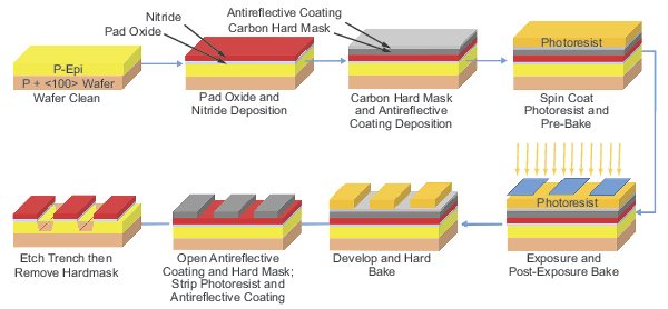
Photolithography, simply put, is the process of "drawing circuits" on a wafer. It's like developing a photograph—the photomask acts as the negative, and the photoresist on the wafer surface acts as the photo paper. By precisely controlling light exposure, the designed pattern is "transferred" onto the wafer. This seemingly simple process is the most critical and most repeated step in chip manufacturing—complex chips can require dozens of layers.
Our Photolithography Process Flow
Step 1: Coating Preparation
A uniform layer of photosensitive material—photoresist—is applied to the wafer surface. This is like turning the wafer into "photo paper." Our automatic spin coater precisely controls the photoresist thickness, ensuring uniformity for subsequent pattern transfer.
Step 2: Alignment and Exposure
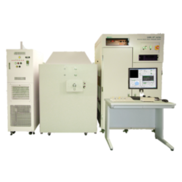
The pattern on the photomask is precisely aligned with existing patterns on the wafer's previous layers, then exposed using specific wavelength light sources. We have multiple exposure tools including DUV (Deep Ultraviolet) for volume production and EBL (Electron Beam Lithography) for high-precision applications, allowing flexible selection based on your requirements.
Step 3: Development
After exposure, a developer solution "washes out" the pattern. Just like photo development, areas exposed to light (for positive photoresist) or unexposed areas (for negative photoresist) are dissolved, leaving a three-dimensional structure corresponding to the photomask.
Step 4: Hard Baking and Inspection
Finally, hard baking enhances the photoresist's resistance during subsequent etching processes, and pattern quality is carefully inspected under an optical microscope.
What We Can Do
Leveraging our 8-inch process platform, we can process various wafer types and pieces, covering:
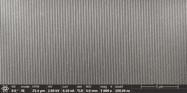
Gratings – Spectral analysis, displacement measurement
Waveguides – Optical communication, sensing
Metasurfaces – Next-gen optical devices
Featured Case: Using small-linewidth metal lift-off process, we successfully fabricated an aluminum grating structure with 100nm thickness and 110nm linewidth, demonstrating high-precision metal patterning capability.
Why Choose Us?
○High Precision: Minimum 8nm linewidth, meeting cutting-edge research needs
○Strong Flexibility: Compatible with 8-inch and smaller wafers of various sizes
○Rich Experience: Successfully fabricated multiple micro/nano structures with mature processes
Please contact Lance at:
sales@plutosemi.com
Bring your designs to life—at the nanoscale.