Lithography Process Services: EBL, DUV & MA6/MA8
If you work with chips or micro/nano devices, you've probably run into this awkward situation:
You finally get a process to work in the lab. Then you try to move it to volume production—and nothing matches. Different tools, different recipes. You have to start over.
Or the opposite: The production line runs stable, but when you want to try something flexible, you're stuck.
What we want to do is build a bridge between these two worlds.
Today, let's talk about the four pieces of our lithography service: EBL, DUV, MA6, and MA8.
Together, they cover the full spectrum—from nanoscale precision work to 8-inch wafer volume production.
EBL: For the Finest Features – The "Nano-Scalpel"
If you're working on single-electron transistors, nanoelectrodes, or any device that requires features at tens of nanometers—you can't avoid EBL.
How it works is straightforward: No mask. A focused electron beam, down to nanometer scale, directly "draws" your pattern on electron-sensitive resist.
Because there's no optical diffraction limit, its resolution isn't bound by light wavelength—it's determined by electron scattering and the molecular size of the resist. That means it can create features finer than any optical lithography.
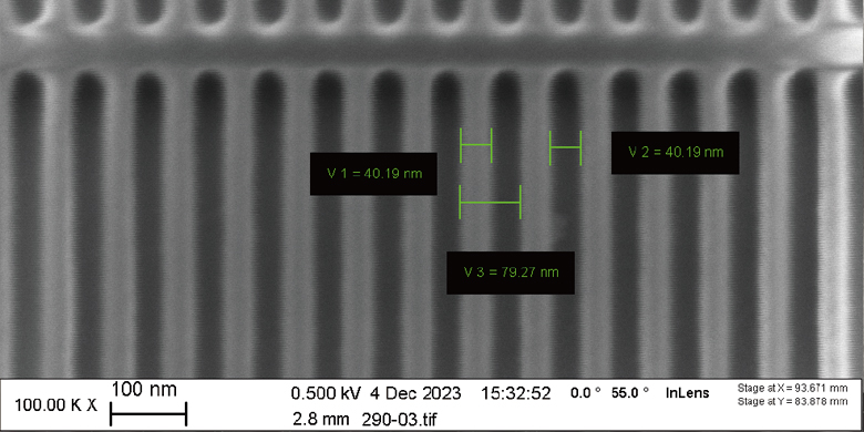
We can reliably deliver 40nm minimum line width—and that's not even the equipment's limit. According to publicly available industry data, advanced EBL systems can achieve minimum feature sizes down to 8nm and grating periods down to 40nm.
We chose 40nm as our stable process node because at this scale, we've fine-tuned all the variables—resist type, electron dose, proximity effect correction—to their most reliable state.
Of course, EBL has a downside: It's slow. Writing a full wafer takes time. It's not for mass production.
But it has one irreplaceable advantage: Flexibility. Want to test a new idea? No need to wait for a mask—just draw it. That's why it's the go-to tool for cutting-edge research and new material exploration.
DUV: From a Few Samples to Thousands of Wafers
When your design works in the lab and you're ready to take it to market—efficiency becomes priority number one.
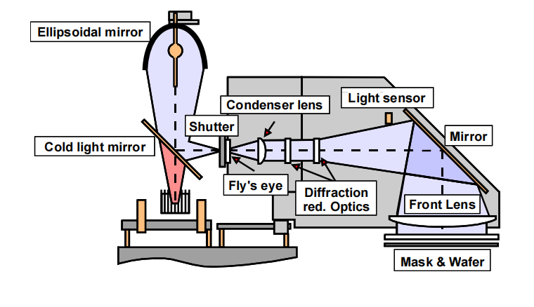
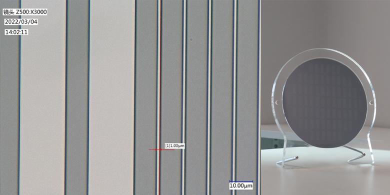
That's when you need DUV—deep ultraviolet lithography. It's the workhorse of semiconductor fabs. Using 248nm deep UV light (KrF source), it projects the mask pattern through high-precision lenses, shrinks it to one-fifth its original size, and steps across the wafer—like a step-and-repeat printer, exposing one field at a time.
We offer 8-inch wafer volume processing. Take the 180nm node as an example—this is the sweet spot for 248nm DUV lithography. With our optimized etch processes, we can reliably reproduce patterns on silicon, wafer after wafer.
According to published equipment specifications, this system achieves overlay accuracy of ≤25nm and resolution down to 150nm or even lower.
And if you're working on silicon photonics—handling specialty materials like lithium niobate or silicon nitride—we've developed processes for those too.
Think of it this way: EBL is hand engraving. DUV is a printing press. When your idea is ready for the world, it's the most reliable tool for the job.
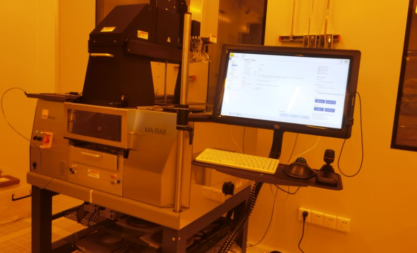
MA6/MA8: Not the Finest, but Reliable and Versatile
Not every device needs nanometer precision.
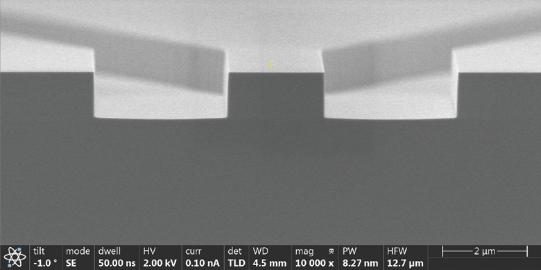
MEMS sensors, power devices, biochips—these typically require line widths in the 0.5μm to a few microns range. But they demand something else: double-side alignment, specialty substrates, and process flexibility. That's where contact lithography shines.
MA6 is our go-to workhorse. It delivers 1μm line width (with ultimate resolution down to 0.8μm). Its superpower is double-side alignment—critical for structures like cantilevers, pressure sensor membranes, and microfluidic channels that need front-to-back pattern accuracy. It achieves backside alignment accuracy within ±1μm.
And it handles 2- to 6-inch pieces, including offcuts and irregularly shaped samples. In R&D, when you're iterating and changing things constantly, it's forgiving and cost-effective.
MA8 is the upgrade. It's compatible with standard 8-inch wafers, maintaining micron-level resolution (down to 0.8μm) while handling higher volumes. With front-side alignment accuracy of ±0.5μm and back-side accuracy of ±1μm, it provides a smooth transition from pilot production to full-scale manufacturing.
What these two tools share: They don't chase the finest line widths. But they adapt well to various materials, thicknesses, and substrate sizes—they're the bridge between R&D and production.
Final Thoughts
From EBL's 40nm precision work, to DUV's 8-inch wafer volume production, to MA6/MA8's reliable versatility at the micron scale—What we offer isn't just a list of equipment specs. It's the experience accumulated behind every process step.
Feel free to reach out if you'd like to discuss.
Let's build better solutions together.
Lance
sales@plutosemi.com