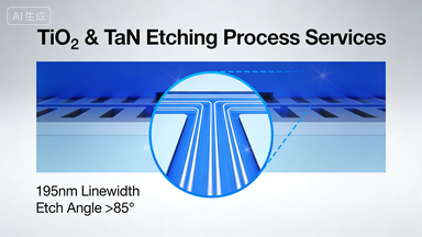
TiO₂ & TaN Etching Process Services: 195nm Linewidth · Etch Angle >85°
What is Etching?
Etching is the pattern transfer step in microfabrication. Simply put, it's about "printing" the pattern from the photoresist onto the underlying material layer
It works a bit like carving: on a wafer that has already been coated with thin films, photoresist acts as a "protective mask," exposing the areas that need to be removed. Chemical or physical methods are then used to "eat away" the material in these areas, eventually leaving the desired pattern on the substrate.
Etching processes fall into two main categories:
Wet Etching
Uses chemical solutions to "dissolve" materials—like using dish soap to remove grease. It's fast and cost-effective, but etching is isotropic, meaning it "undercuts" beneath the material, limiting precision.
Dry Etching
Uses plasma or ion beams to "bombard" the material—like sandblasting glass. It allows directional control, achieving near-vertical sidewalls, making it ideal for high-precision patterns.
The etching process services we provide are based on dry etching technology, meeting the demands of high aspect ratio and high verticality processing.
Our Etching Process Capabilities
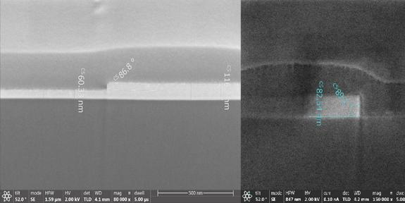
Etching of metasurface optical structures requires precise control over aspect ratio and sidewall verticality. Tantalum nitride (TaN) is commonly used as a hard mask for fused silica etching, where control of the etch angle directly impacts pattern transfer accuracy.
Sharing two sets of recently validated process data:
Titanium Dioxide (TiO₂) Meta-Structure Etching
Linewidth: 195nm
Depth: 650nm (aspect ratio ~3.3:1)
Applications: Metalenses, polarization control devices
Tantalum Nitride (TaN) Etching
Compatible substrates: Silicon, fused silica
Etch angle: >85° (near vertical)
Applications: Thin film resistors, hard mask layers, optical attenuators
We Offer More Than Just Equipment
We provide process solutions and foundry services that have been practically validated. From university research groups to corporate R&D centers, if you're looking for reliable TiO₂ or TaN etching support, feel free to reach out for a discussion
Contact:
Lance Xie
sales@plutosemi.com