Process Testing Services
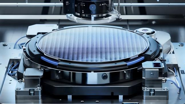
Have you ever wondered that in a chip the size of a fingernail, there are circuits as complex as a city's transportation network? When these circuits experience "traffic jams" or "road breaks," how do we pinpoint the problem?
In the micro-world, we need to find defects just tens of nanometers in size—on a scale one-thousandth the diameter of a human hair. It's like looking for a grain of sand in a football field—and this is what we deal with every day.
In our daily work, we rely on these tools to "see" and "dissect" the micro-world:
Scanning Electron Microscope (SEM) — the "first eye" into microstructures. The invisible surface details of a chip appear on the screen, revealing the outlines of precision circuits with clarity.
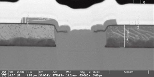
Dual-Beam Microscope (FIB-SEM) — think of it as a precise "light knife." When we need to find the root cause of a chip failure, we use it to slice through structures layer by layer. Combined with EDS analysis, we not only locate the defect but also identify its composition.
When it's time to prepare TEM samples, the FIB becomes a "micro-carving tool." It carves out thin slices—less than 100 nanometers thick—from exact locations. This requires extreme precision, and it's something our engineers are quite familiar with.
Atomic Force Microscope (AFM) — used to sense surface variations. It maps out the three-dimensional "terrain" of materials with atomic-level precision, quantifying roughness and step heights accurately.
As for Film Thickness Testers and Ellipsometers, they're mainly used for "checkups" on thin films. Without contact or damage, they measure film thickness and optical properties (refractive index n, extinction coefficient k). Sometimes a film looks uniform, but only after measurement do we know if the parameters are within spec—that sense of certainty, anyone in process work understands.
Currently, we have access to these tools:
Dual-Beam Microscope & FIB-SEM/EDS
High-Resolution SEM
Metallurgical/Digital Microscope
Atomic Force Microscope
Ellipsometer, Stylus Profiler, Film Thickness Tester
From routine morphology observation to failure analysis and TEM sample preparation—if you have related needs, feel free to reach out.


