Over the past few years, processor compute power has skyrocketed, but memory data transfer speeds have lagged significantly behind. This widening chasm between compute and data throughput is known as the "Memory Wall." When a GPU is left starving for data, infinite compute power is useless.
The advent of HBM (High Bandwidth Memory) completely changed the game. Instead of merely increasing clock speeds, it achieves an exponential leap in data throughput by "widening the highway," making it an absolute necessity in the era of Large Language Models (LLMs).
The Core Tech: A Manufacturing Marvel of 3D Stacking & TSV
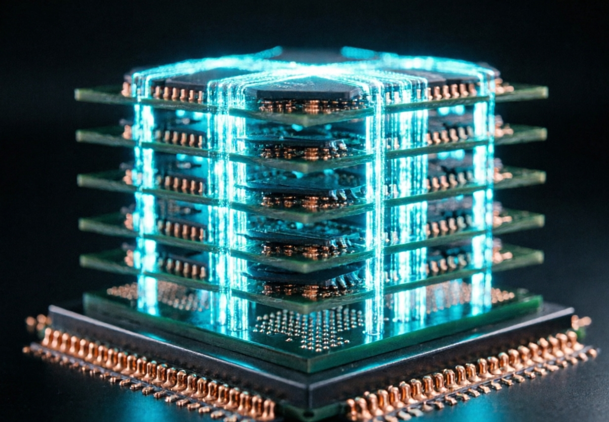
At its core, HBM is not a single memory chip; it is an incredibly complex 3D integrated micro-system . Its manufacturing difficulty makes it a crown jewel of semiconductor processing:
Through-Silicon Via (TSV): Manufacturing HBM requires etching tens of thousands of microscopic holes through ultra-thin DRAM dies and filling them with copper for vertical conductivity. This demands extreme High Aspect Ratio Etching (HARC) and perfect thin-film deposition. A single via defect ruins the entire HBM stack.
Microbumps & Ultra-Thin Wafer Handling: 8 or even 12 layers of DRAM wafers are thinned to extreme limits, then vertically compressed using microbumps. Controlling thermal stress and warpage on such fragile materials is the ultimate test for packaging engineers.
The Bottleneck: The 2.5D Advanced Packaging Choke Point
Manufacturing the HBM stack is only step one; connecting it to the GPU is the real industry bottleneck.
Today's high-end AI chips universally adopt 2.5D advanced packaging (like TSMC's CoWoS) . The GPU and HBM must be placed side-by-side on a highly expensive "Silicon Interposer." As the demand for HBM capacity surges (eg, from HBM2E to HBM3E), the interposer area expands, aggressively consuming a fab's masking and etching capacity. This is the root cause of the AI chip shortage.
Looking Ahead: The Bumpless HBM4 Era
To further boost bandwidth and reduce power consumption, the upcoming HBM4 will trigger another manufacturing revolution. The industry is aggressively pushing Hybrid Bonding technology, aiming to eliminate microbumps entirely and achieve direct copper-to-copper connections between wafers.
In an era where compute is power, whoever masters the yield of top-tier 3D stacking and advanced packaging holds the throat of the global AI supply chain.