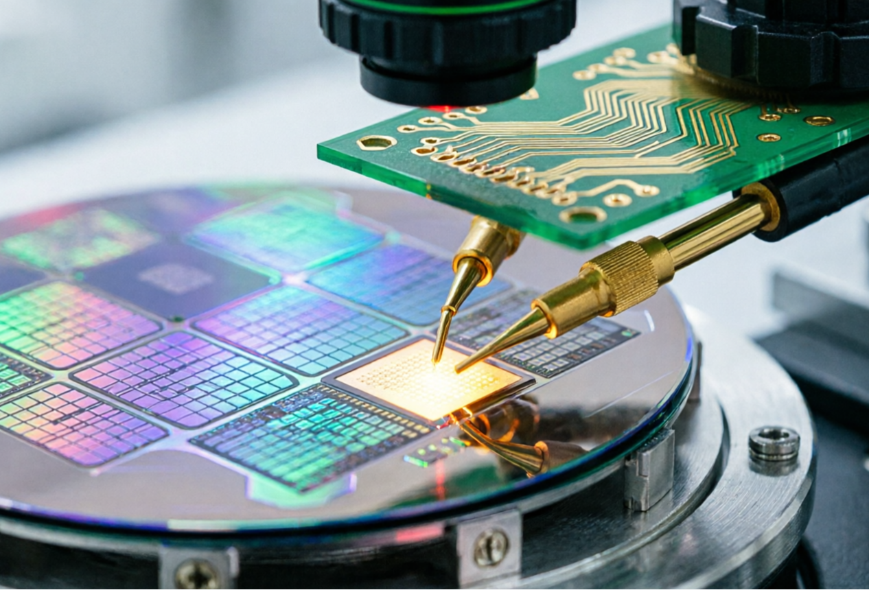
Micro-Nano Foundry: 5 Key Steps from Wafer to Die
1. Wafer Preparation
High-purity silicon ingots are sliced, ground, and polished into mirror-like wafers, the "foundation" for all circuits.
2. Photolithography
The core step. Using a lithography machine to "print" circuit patterns onto the photoresist-coated wafer with nanometer precision.
3. Etching & Implantation
The real "carving" begins. Etching removes excess material, and ion implantation alters silicon's conductivity to build the transistor's 3D structure.
4. Wafer Probing
Before dicing, a prober tests every single Die on the wafer. Only electrically qualified chips are marked to proceed.
5. Thinning & Dicing
The wafer's backside is ground thin, then sliced into individual units—this is what we call the Bare Die.
These dice are typically delivered in Waffle Packs or Tape & Reel