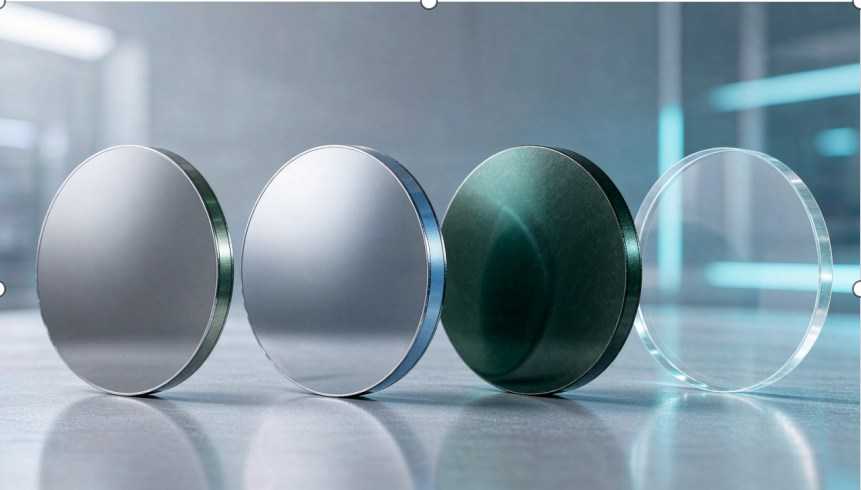
A chip’s performance ceiling is set the moment its substrate is chosen. Silicon, SOI, SiC, fused silica... they are not mere "raw materials" — they are the first building block that decides your process route, cost, and yield ceiling. Let’s discuss: when choosing a substrate, do you prioritize purity, lattice match, or cost?
Why the Substrate Comes First
Chip manufacturing is like erecting a skyscraper on sand — a weak foundation makes any advanced process upstairs pointless. The substrate IS that foundation: every deposition, lithography, and etch step happens on it, and its lattice, flatness, and thermal stability directly determine device performance and yield ceiling.
Mainstream Substrates, Each with Its Own Arena
Silicon (Si): the undisputed home of logic and memory — the most mature supply chain at the lowest cost.
SOI wafers: buried-oxide isolation makes them the weapon of choice for silicon photonic modulators, RF devices, and low-power chips.
SiC / GaN substrates: the energy arena of wide-bandgap semiconductors — the power core of EVs and fast charging.
Fused silica (e.g., JGS1) and sapphire: the transparent arena for optics and specialty devices — from DUV optics to LED substrates.
Substrate Structure Comparison
My Take
Substrate selection is the most underestimated process decision. Engineers obsess over lithography and etching, yet forget: changing the substrate means changing the process route. Lattice mismatch, thermal expansion differences, surface defects — any one of them can scrap an entire wafer lot. Choose right, and you win at the starting line; choose wrong, and you are running the most expensive trial-and-error on the most expensive equipment.
Conclusion
As chip scaling approaches physical limits, the industry’s gaze is shifting from "process" to "materials." Whoever master's the behavior of the substrate holds the ticket to next-generation devices.